
Refractive Index Data
Efficiency optimization of tandem QLEDs
ContributorYuhan LI
Very Stable and Efficient Tandem Quantum-Dot Light-Emitting Diodes Enabled by IZO-Based Interconnecting Layers Cuixia Yuan, Zinan Chen, Fengshou Tian, Shuming Chen*
Highlights
This research developed a novel Tandem QLED structure. From an electrical perspective, through a combination of simulation and experimental work, an interconnecting layer (ICL) based on indium zinc oxide (IZO) and conductive ZnMgO was designed, significantly reducing the driving voltage of the Tandem QLED. Optically, by developing a top-emitting structure (TE) and optimizing the cavity length guided by optical simulations, maximum light extraction efficiency (LEE) was achieved. The optimized Tandem QLED exhibited a maximum external quantum efficiency of 49.01% at 1000 cd/m2 with a T95 lifetime exceeding 50,000 hours, making it one of the most efficient and stable QLEDs reported at the time of publication.
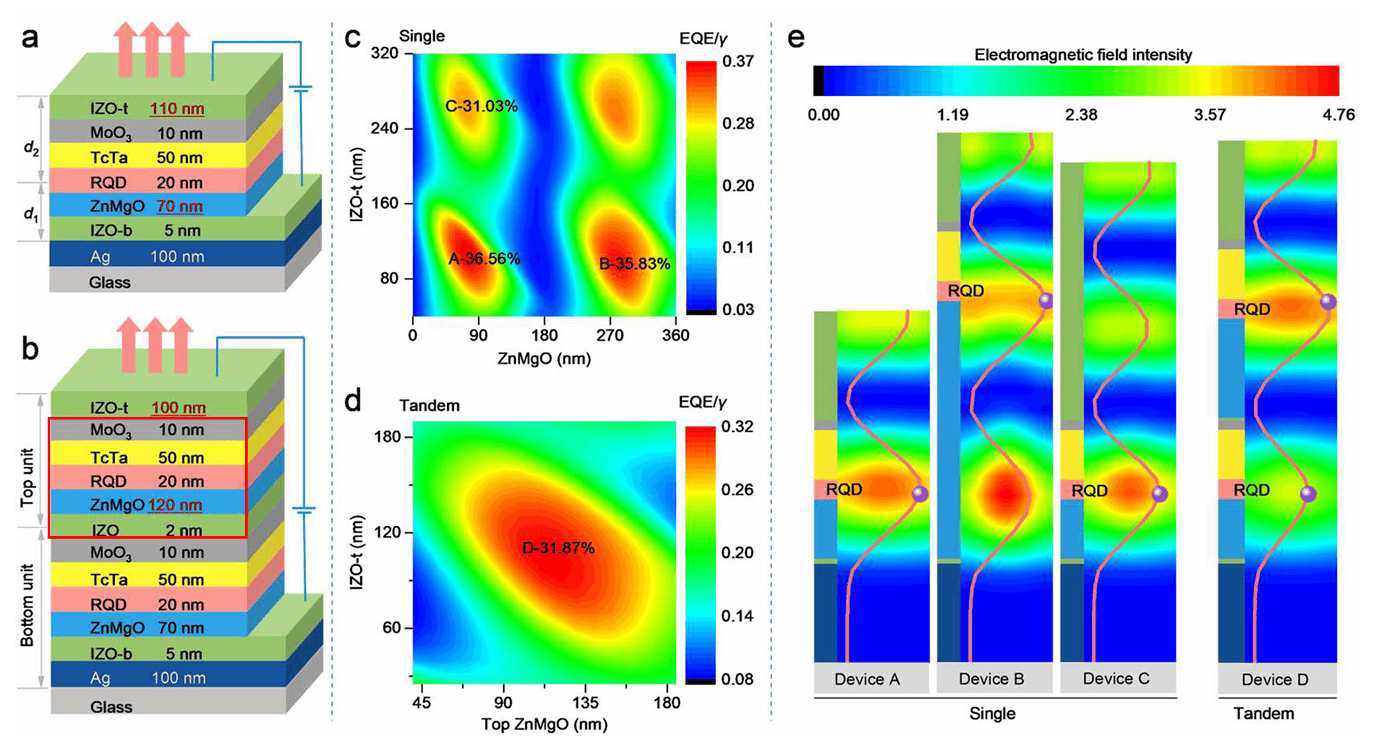
Figure 2: Optical design of Tandem QLEDs. (a) and (b) show the optimized structures of single-emission-layer and tandem devices, respectively. (c) and (d) show the simulated EQE/γ values for single-emission-layer and tandem devices, respectively. (e) shows the calculated electromagnetic field distribution for the devices marked in (c) and (d).
Reprinted with permission from Yuan et al., Nano Letters. Copyright 2024, American Chemical Society.
Preparation
Following the Installation and Licensing guide, ensure Leda is properly installed and activated.
The authors provided refractive index data in Figure S5 of the Supporting Information.
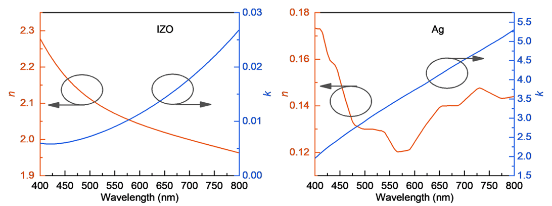
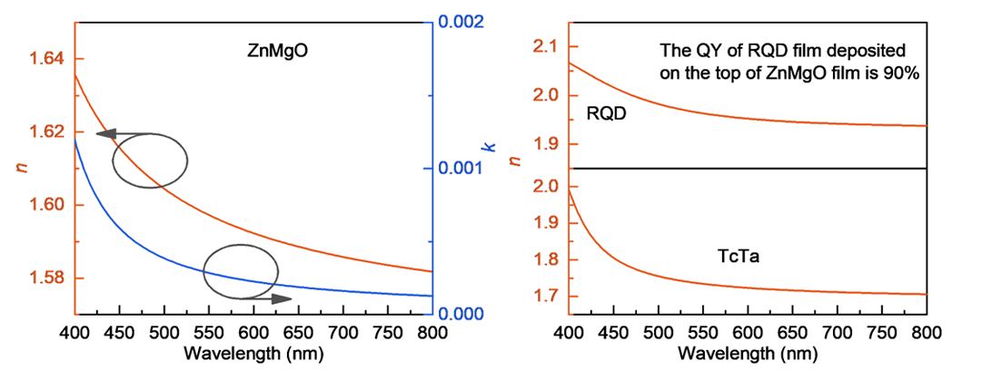
Figure S5: Parameters used for simulating EQE/γ and electromagnetic field distribution. Additionally, the authors set the refractive indices of MoO3 to be the same as those of TcTa in the simulation (as stated in the Supporting Information: “the refractive indices used for MoO3 are the same as those of TcTa”).
Reprinted with permission from Yuan et al., Nano Letters. Copyright 2024, American Chemical Society.
Download the following data extracted from Figure S5 to your local machine.
Spectral Data
This data is provided solely for this case study. If you intend to use this data for actual projects, please cite: Yuan et al., 2024
Simulation Validation
We will use Leda to reproduce the simulation results shown in Figure 2.
Single-Emission-Layer Device
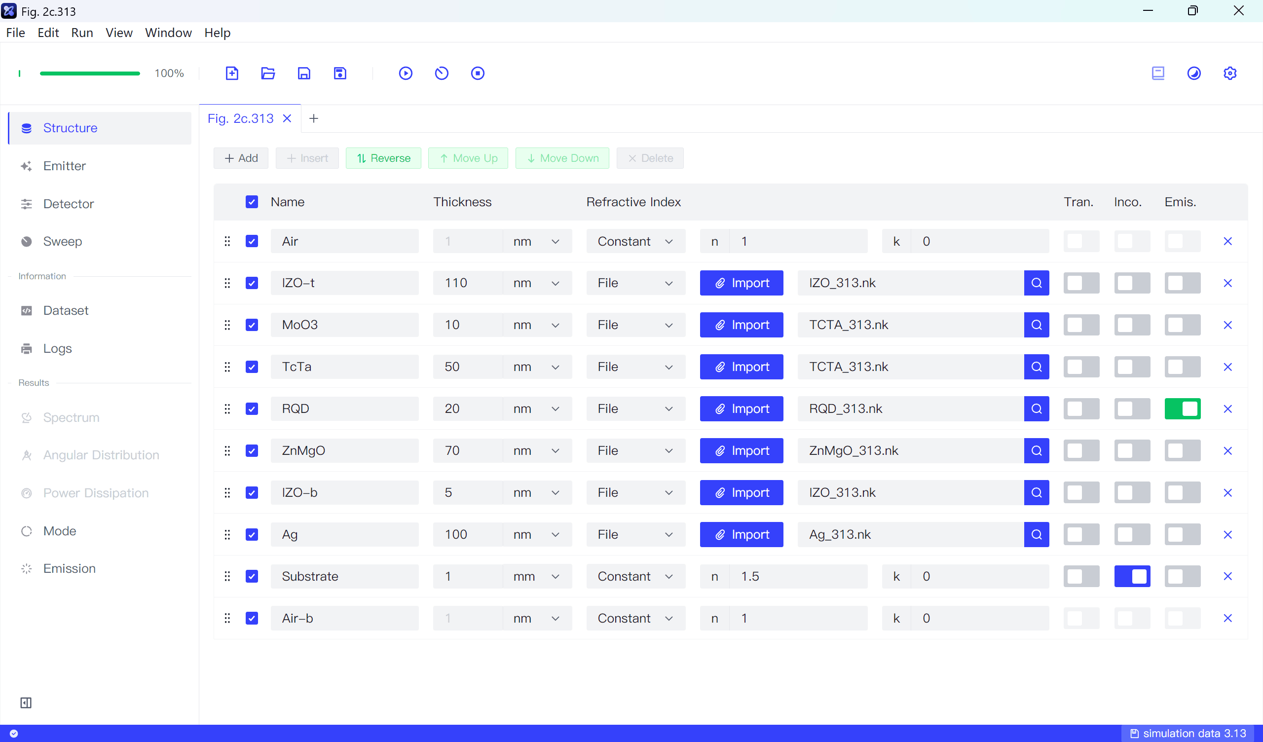
First, we’ll build a conventional single-emission-layer TE-QLED structure according to Figure 2(a), importing the refractive index data provided by the authors for each layer. As noted in Figure S5, the refractive indices used for MoO3 are the same as those of TcTa, so we can import the same file.
Activate the Emis. property for the RQD layer to designate it as the EML; since the substrate is 1 mm glass, activate the Inco. property for the Substrate.
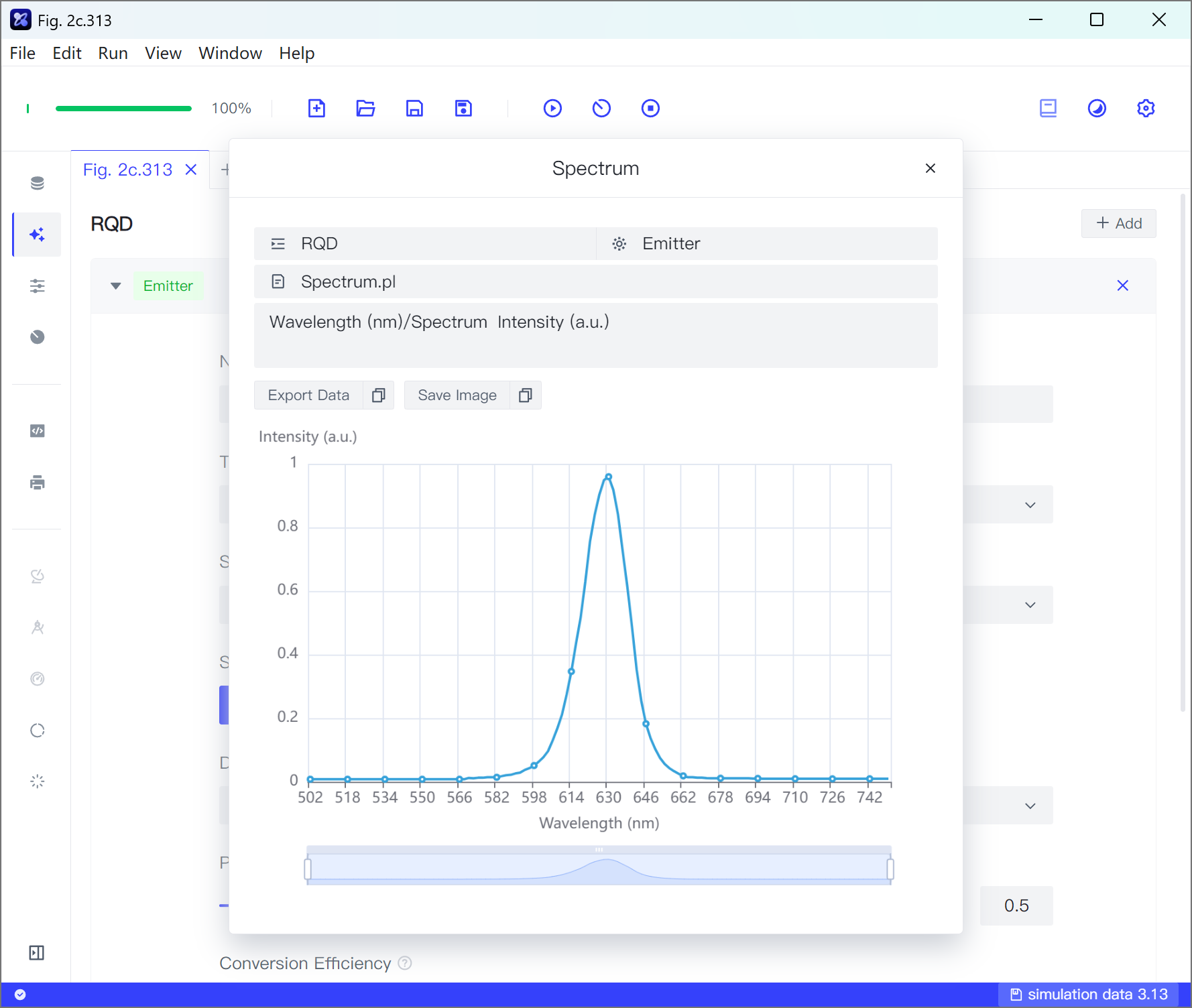
In the Emitter settings, import the PL spectrum provided by the authors in Figure S1.
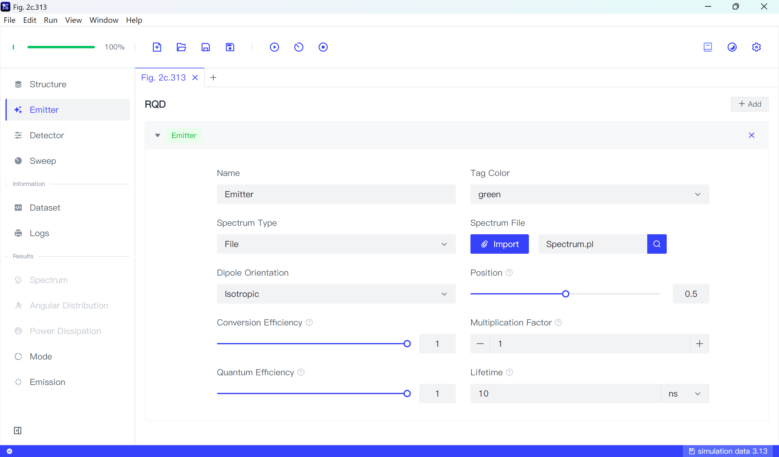
Examine the imported PL spectrum, which has an effective wavelength range from 590 to 670 nm.
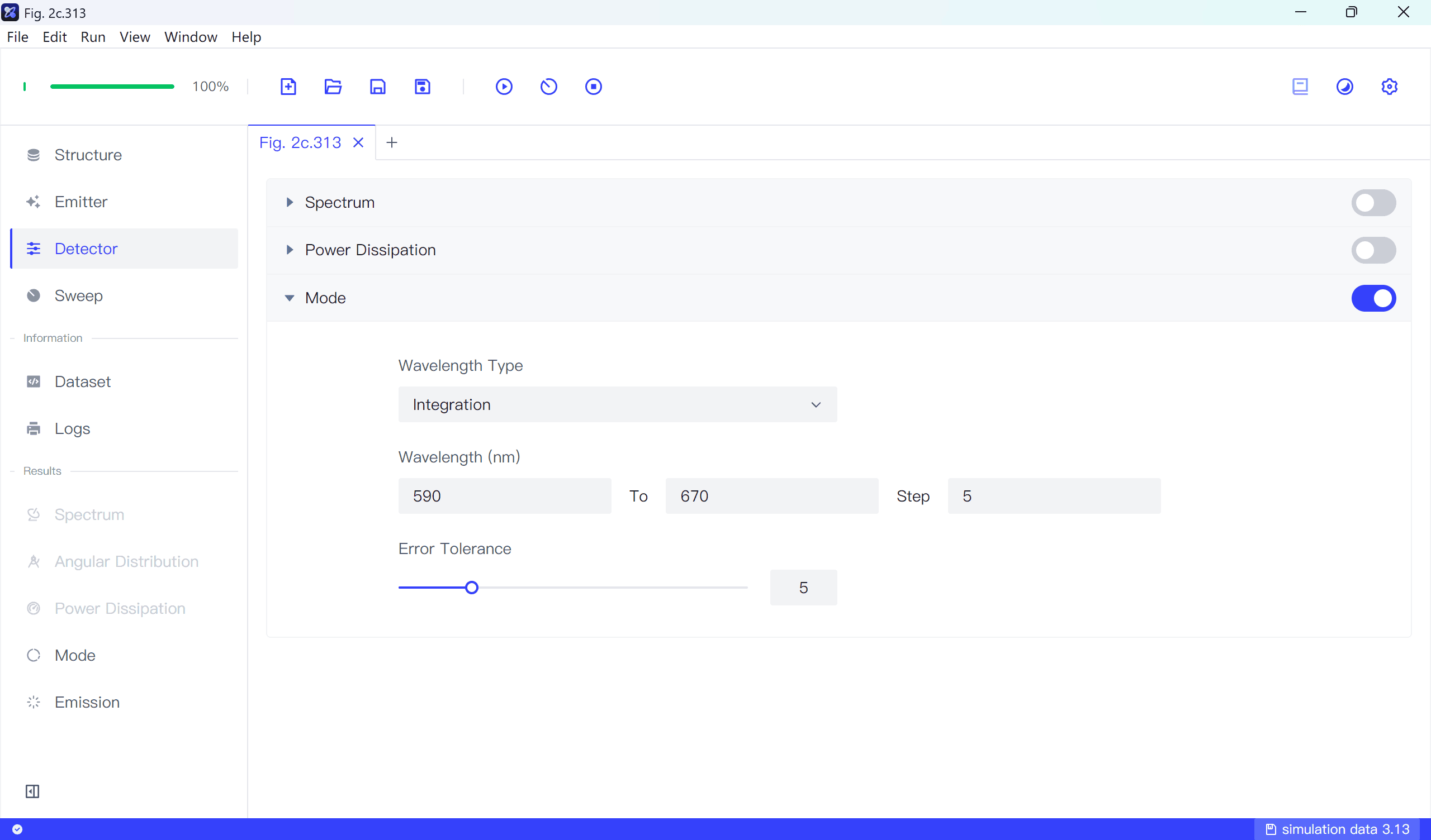
Enable the Mode Detector and set the Wavelength Type to Integration. Based on the Emitter’s spectral range, set the Wavelength range from 590 nm to 670 nm with a Step of 5 nm.
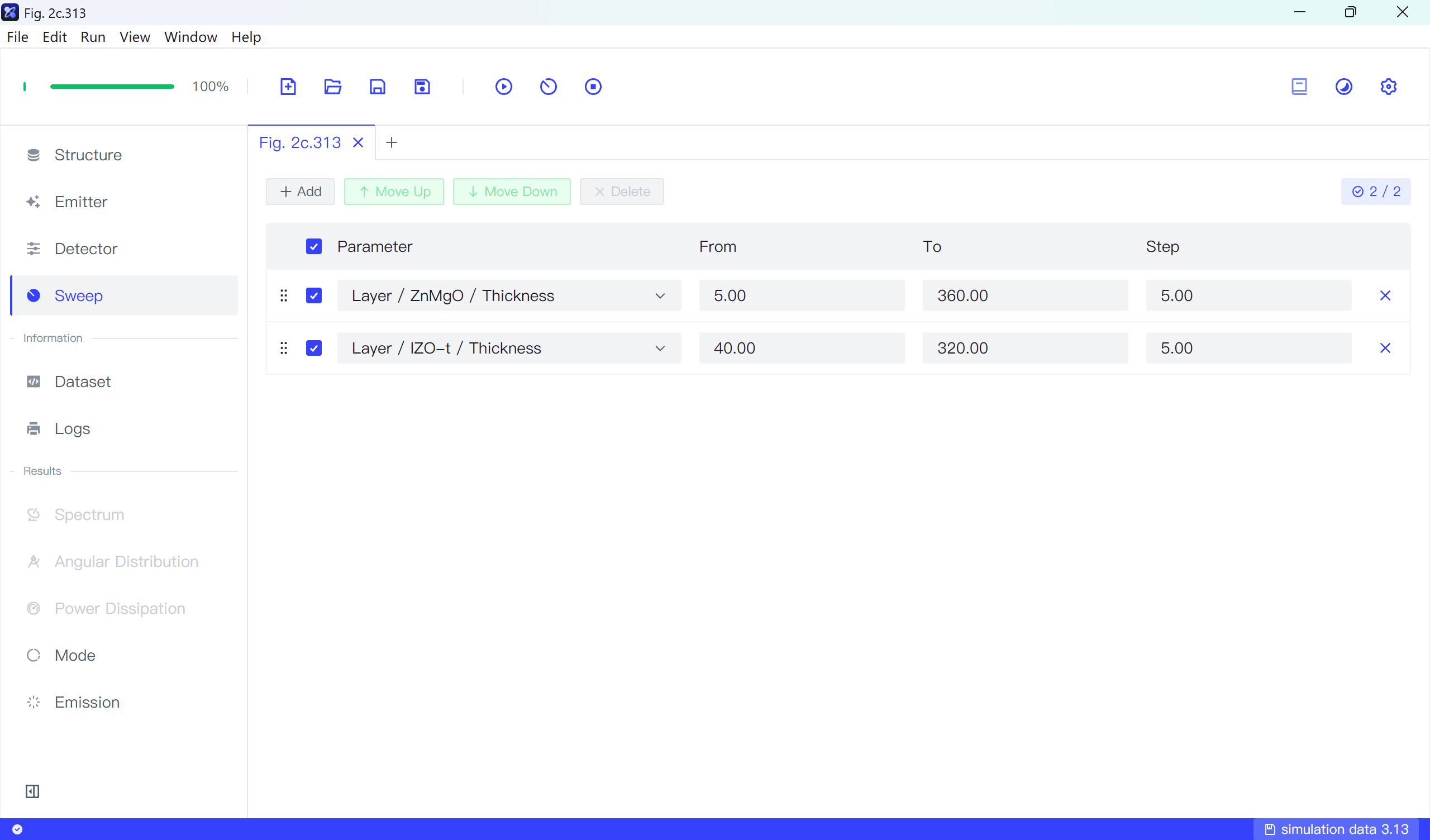
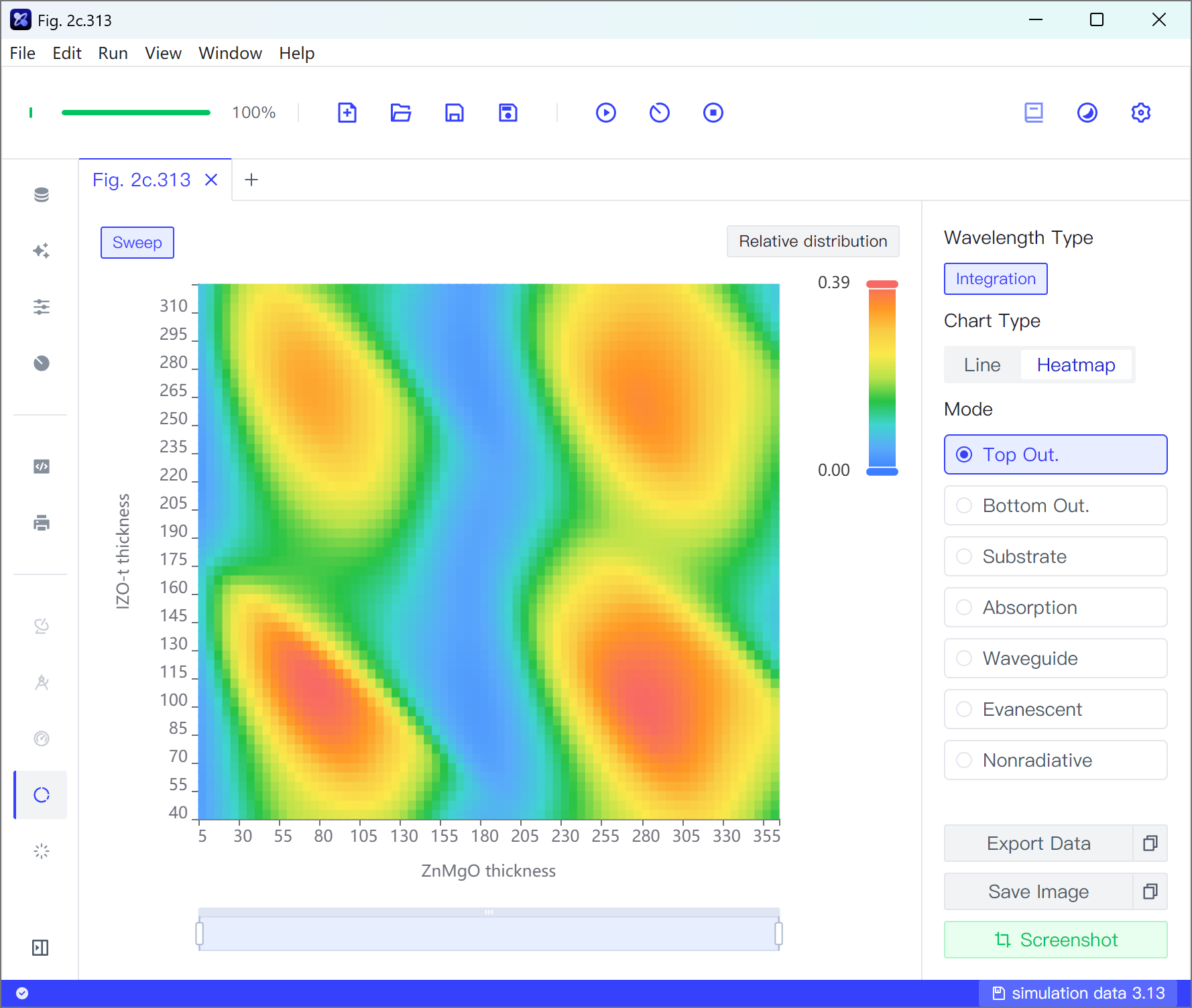
In the Sweep settings, add layer thickness scanning: set ZnMgO thickness from 5 nm to 360 nm with a step of 5 nm; set IZO-t thickness from 40 nm to 320 nm with a step of 5 nm (you can further increase precision, but this will extend computation time).
Click Run Sweep to obtain the scan results. In the Mode section, switch the Chart Type to Heatmap to observe how EQE varies with ZnMgO and top IZO thickness. As shown below, we’ve reproduced the same pattern as in Figure 2(c).
Tandem Device
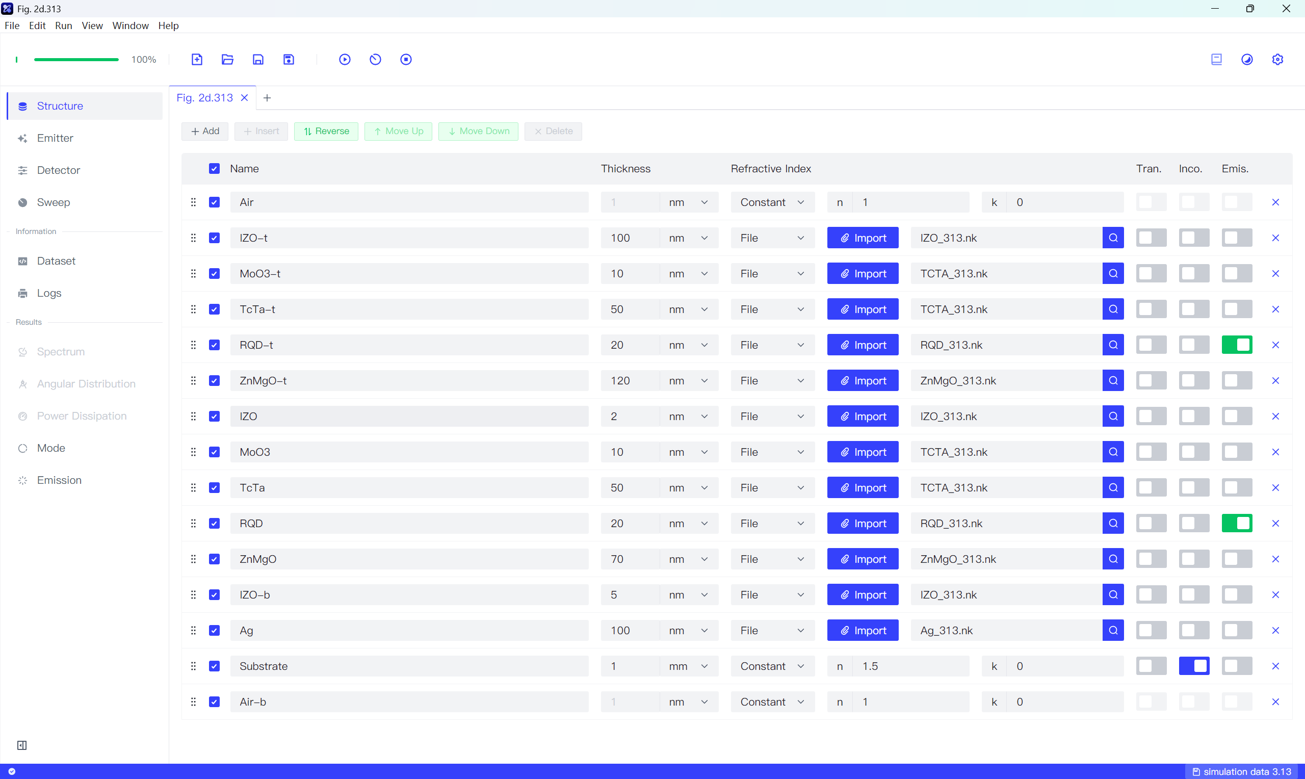
Next, we’ll build a Tandem TE-QLED device structure according to Figure 2(b), importing the refractive index data provided by the authors for each layer. Again, following the original description, we’ll import the same file for MoO3 as for TcTa. Activate the Emis. property for both RQD-t and RQD layers to designate them as EMLs; activate the Inco. property for the Substrate.
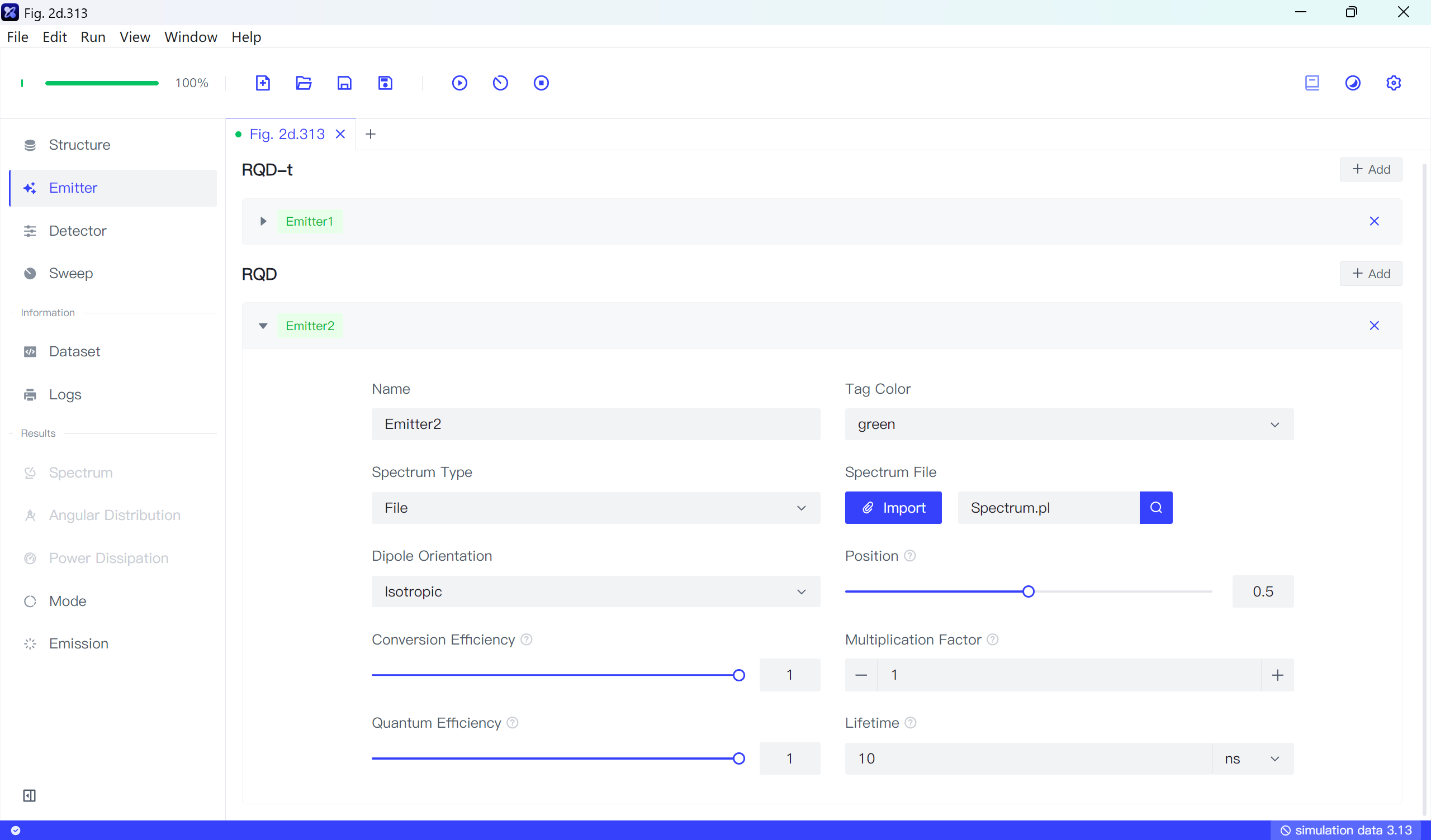
According to the original text: “In the optical design of a tandem QLED, it is assumed that the charge balance factors or electrical efficiencies of the two emitting units are equal.” In the Emitter settings, create identical parameters for Emitter1 and Emitter2 for RQD-t and RQD respectively, importing the RQD spectrum Spectrum.pl provided by the authors for both.
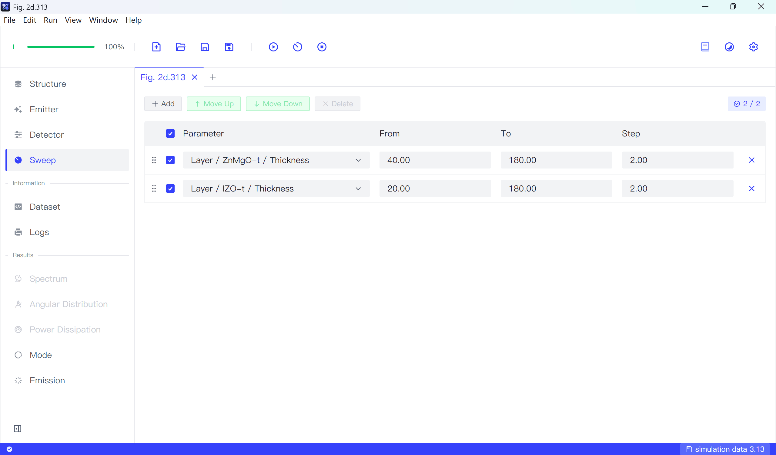
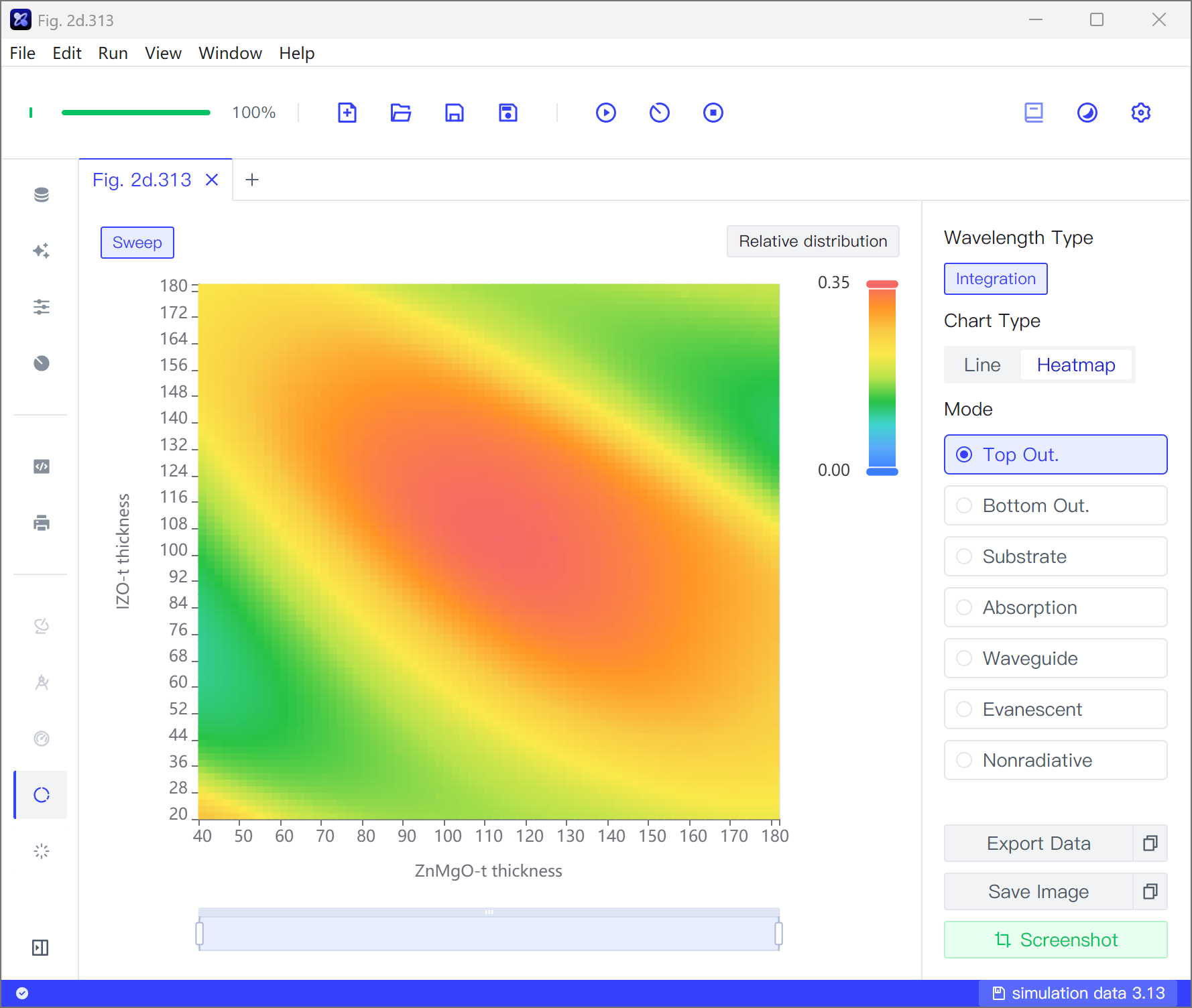
Maintain the Mode Detector settings and add layer thickness scanning in the Sweep: set ZnMgO-t thickness from 40 nm to 180 nm with a step of 2 nm; set IZO-t thickness from 20 nm to 180 nm with a step of 2 nm.
Click Run Sweep to obtain the scan results. As shown below, we’ve reproduced the same pattern as in Figure 2(d).
Conclusion
This case study demonstrates the development of a Tandem QLED with a top-emitting structure and optimized cavity length, achieving maximum light extraction efficiency and ultimately resulting in a highly efficient QLED.
By modeling the device in Leda and using the data provided in the paper for simulation calculations, we obtained results nearly identical to those in the paper, quickly completing a professional optical simulation validation.
Return