Sweep and Optimization
Sweep is a key function for exploring optical mechanisms and optimizing device parameters. This section introduces the use of the Sweep and methods for device optimization.
Sweep
Leda’s sweep setup is straightforward. Simply configure the sweep items in the Sweep menu and click Run Sweep in the toolbar to complete the sweep.
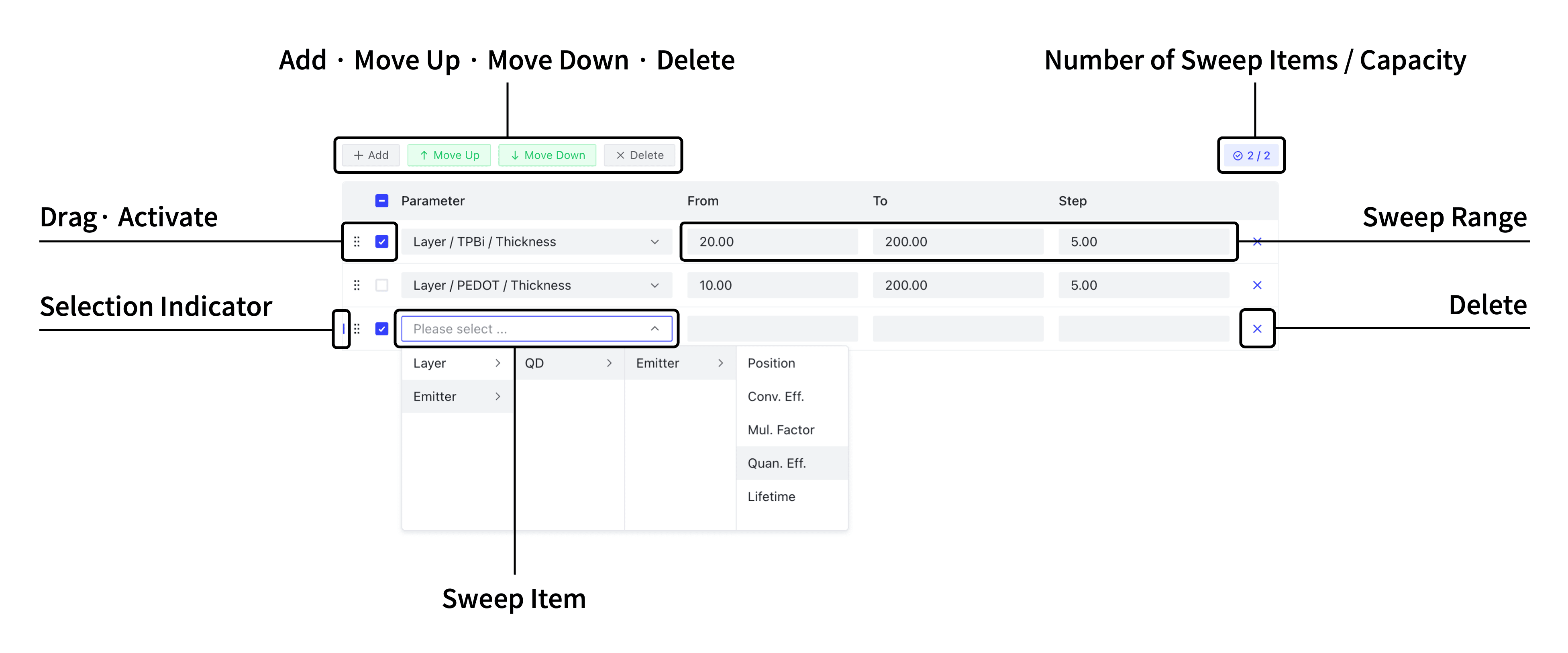
Click Sweep in the sidebar to enter the sweep setup interface, as shown below:
Operating Sweep Items
At the top are tools for operating sweep items, which can be used to add, move up, move down, or delete sweep items.
Move Up, Move Down, and Delete are unavailable when no sweep item is selected. You need to click on a sweep item to select it before operating. Once selected, a blue indicator appears on the far left of the sweep item, indicating the currently selected item.
- Adding Sweep Items: Click
Addto add a sweep item at the bottom. - Sorting Sweep Items: In addition to using
Move UpandMove Downwhen a layer is selected, you can also drag the⋮⋮symbol on the left to sort. - Deleting Sweep Items: Select a layer and click
Deleteto remove it, or click the⨉on the far right of the sweep item to delete it.
Configuring Sweep Items
Click the Parameter section of a sweep item to select the target parameter in the cascading selector. For example, select Layer/PEDOT/Thickness to sweep the thickness of the PEDOT layer; select Emitter/QD/Emitter/Quan. Eff. to sweep the intrinsic quantum efficiency of the emitter named Emitter in the QD emitting layer.
Enter the sweep range in From, To, and Step. For example, entering 10, 200, 5 in the Layer/PEDOT/Thickness item means the thickness of the PEDOT layer will increase from 10 nm to 200 nm in 5 nm intervals.
The following specifications apply to sweep item configuration:
- Units are determined by the settings in Structure, and the sweep only modifies values without defining units.
- The sweep range must be greater than 0 and increasing,
Stepmust be positive, and the number of sweep points must not exceed 200 to avoid excessive computation. - Precision is to two decimal places.
Sweep Capacity
The sweep capacity is 2, meaning only 2 sweep items can be used at a time. The upper right corner of the sweep configuration interface displays Number of Sweep Items/Current Available Capacity. When the number of sweep items exceeds the current available capacity, an orange warning appears, and the error status bar at the bottom of the software turns orange.
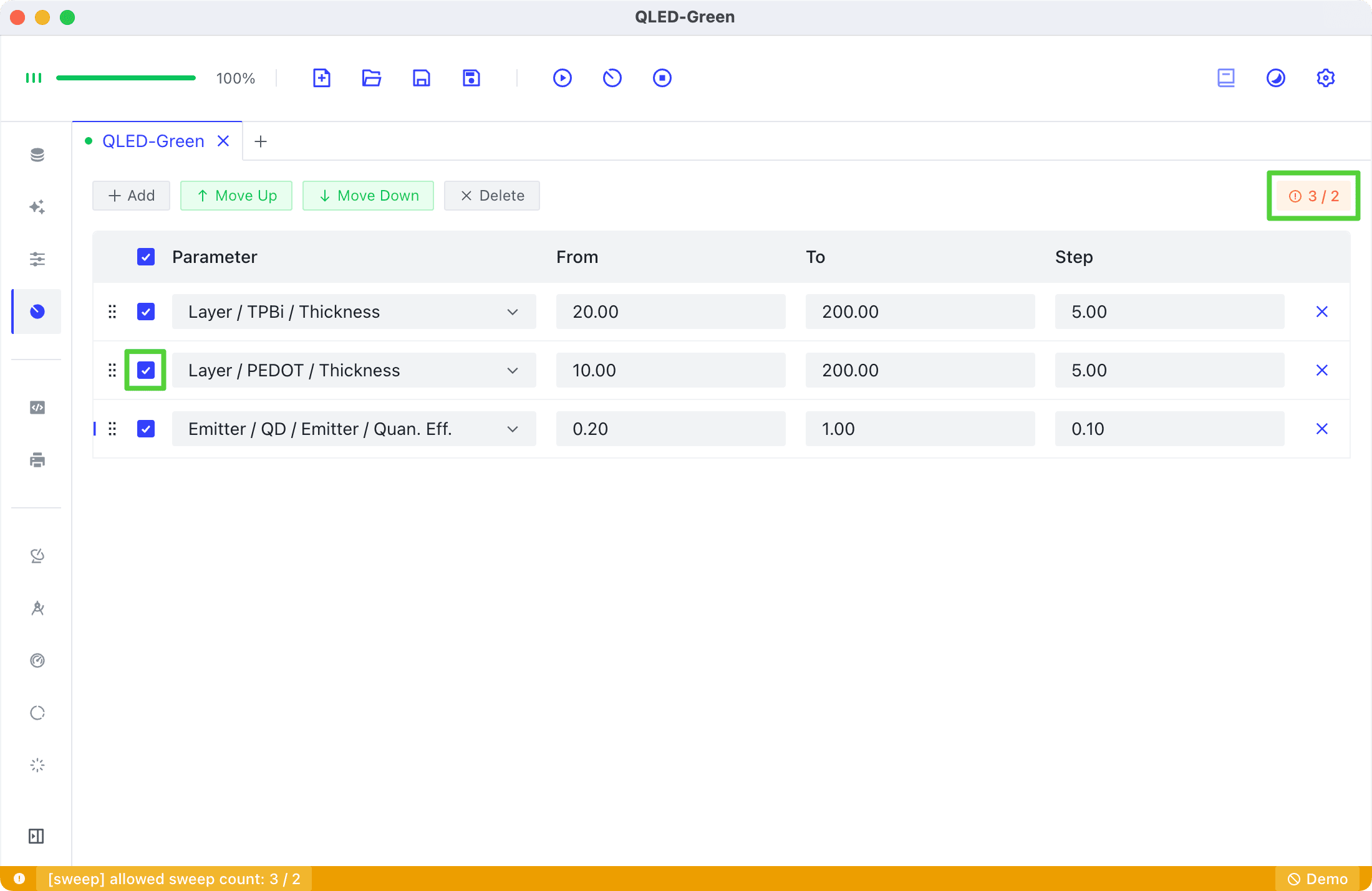
You can close sweep items by unchecking them without deleting them.
Why only 2 sweep items are allowed
- Two-dimensional charts can only display two-dimensional data.
- Storing and processing three-dimensional data is challenging and computationally intensive.
Although the sweep capacity is limited to 2, more parameters can still be optimized through multiple sweeps based on optical principles.
Detector Occupying Sweep Channels
Sometimes the sweep capacity is not 2, but 1 or even 0, as shown below.
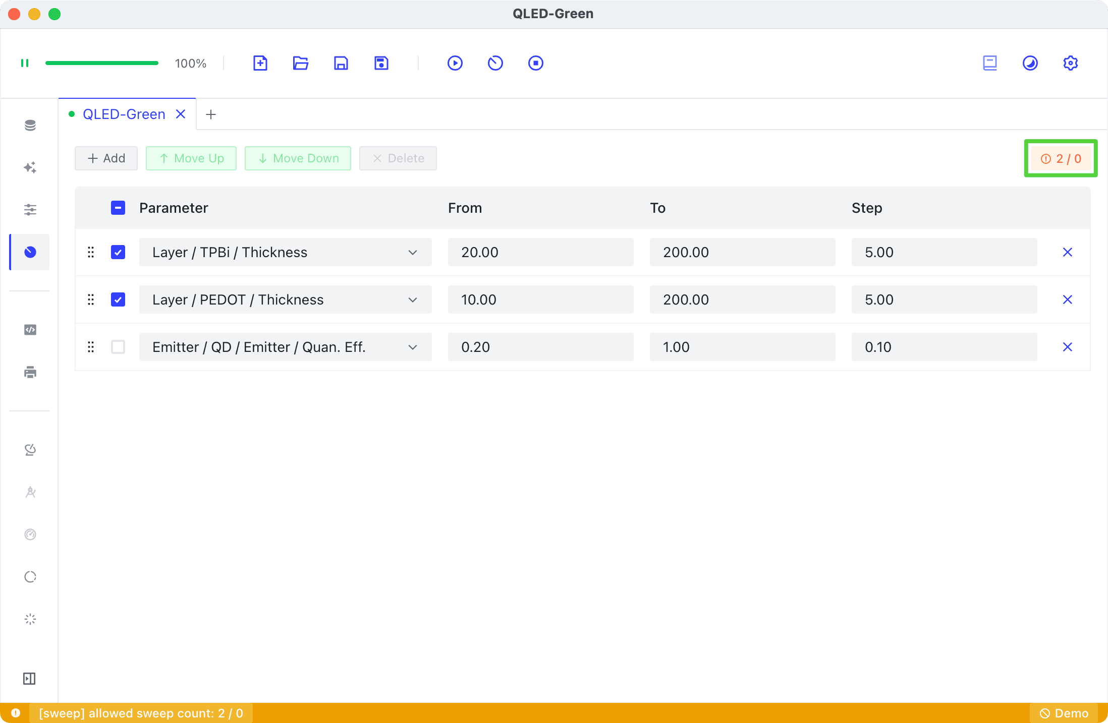
This is because the Detector occupies sweep channels.
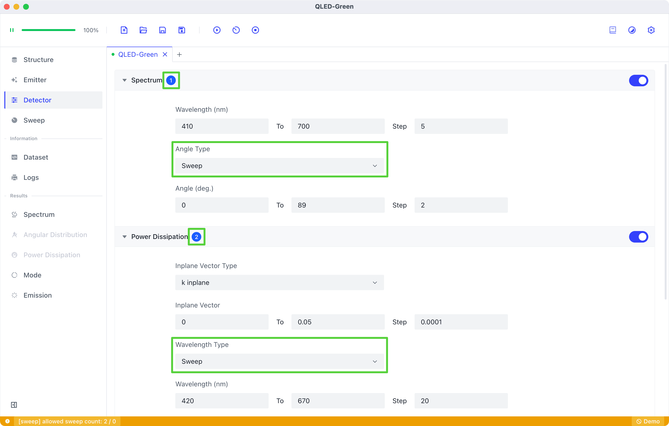
For example, when the Angle Type of the Spectrum detector is set to Sweep, it occupies 1 sweep channel, and when the Wavelength Type of the Power Dissipation detector is set to Sweep, it occupies 2 sweep channels.
In this case, among the enabled detectors, Power Dissipation occupies the most sweep channels, which is 2, so the available sweep capacity is 2-2=0.
Optimization
Efficiency Optimization of Microcavities
According to the principles of the Microcavity Effect, the microcavity is regulated by the distance between the dipole and the reflector (especially the metal reflector) and the cavity length. Specifically, efficiency is related to the following parameters:
- HTL thickness
- ETL thickness
- EML thickness
- Position of the dipole in the EML
For structures with only a single metal electrode, first optimize the distance between the Emitter and the metal electrode. For example, in the Air/Substrate/ITO/PEDOT/QD/TPBi/Al/Air structure, prioritize optimizing the thickness of TPBi, followed by PEDOT.
The Mode detector can most intuitively observe LEE optimization, so only the Mode detector is activated in the Detector, configured as follows:
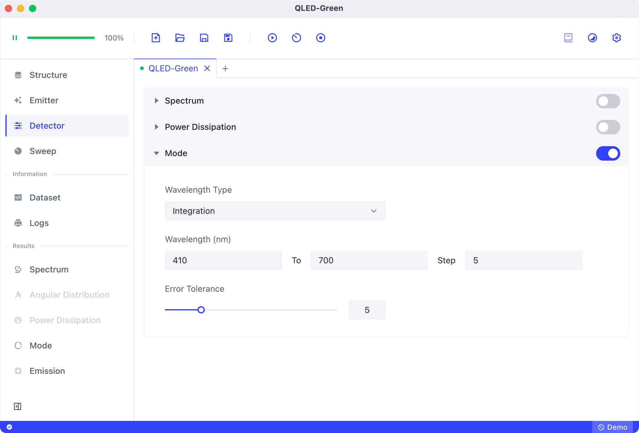
Configure the thickness sweep of TPBi and PEDOT in Sweep:
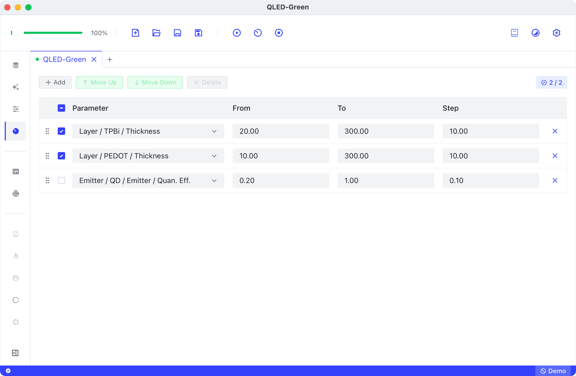
Click the Run Sweep button in the toolbar and wait for the progress bar to reach 100% to complete the simulation.
Periodic Changes
Click Mode in the sidebar, switch Chart Type to Heatmap in the right settings to view the changes in each Mode with the sweep items (click the video below to play).
Select Top Out. in Mode, and observe in the results that LEE is affected by the thickness of TPBi and PDEOT, showing periodic changes.
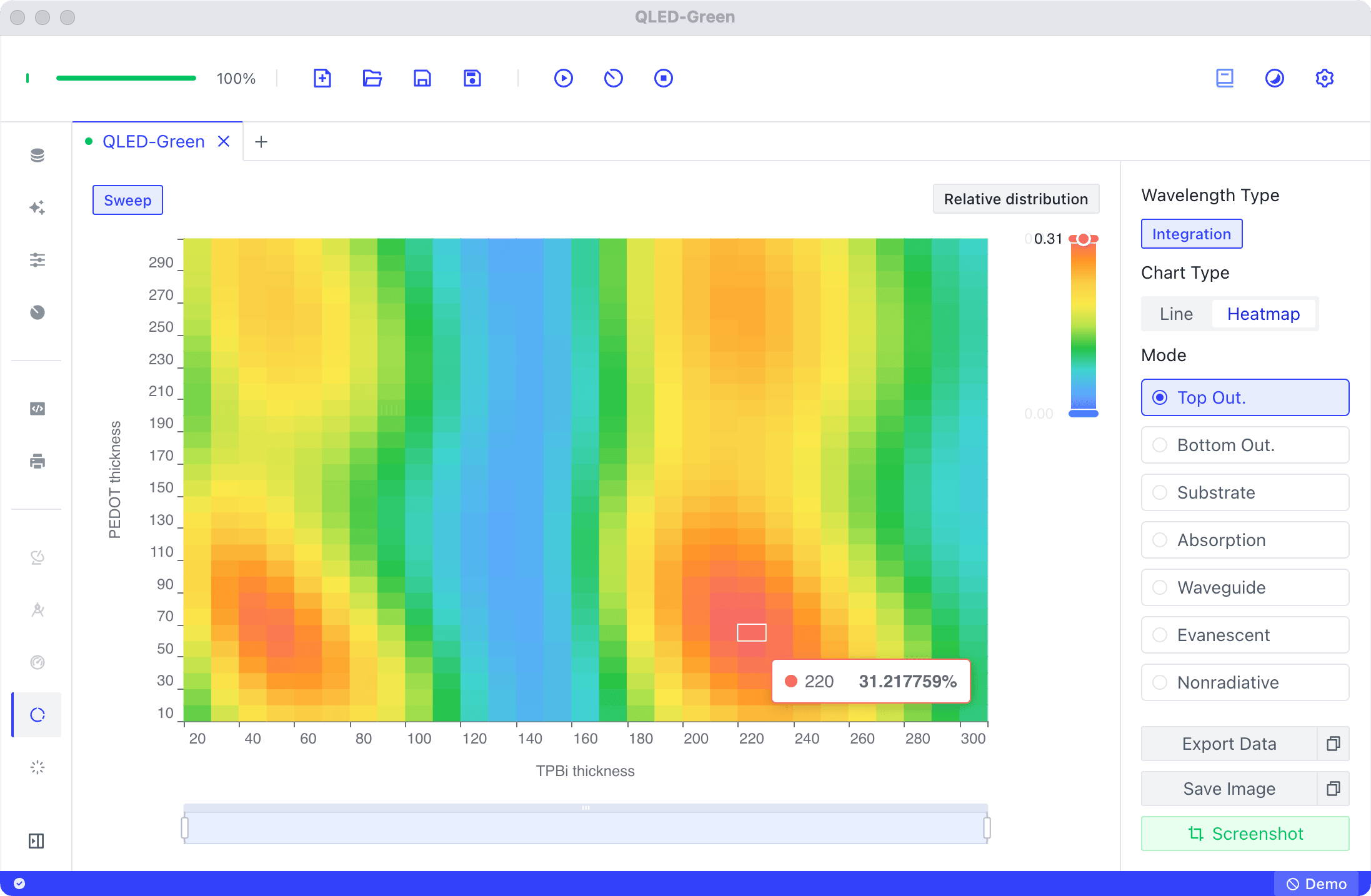
The fluctuations in LEE with TPBi thickness are larger, while those with PEDOT thickness are smaller. This is consistent with the Microcavity Effect, as TPBi thickness dominates wide-angle interference and regulates multiple-beam interference.
With TPBi thickness at 220 nm and PEDOT thickness at 60 nm, the optimal LEE reaches 31.22%. However, due to the limitations of the electrical properties of the material, TPBi at this thickness affects charge transport, so this thickness is not practically chosen. Therefore, TPBi thickness can be selected in the range of 40–50 nm, and PEDOT thickness in the range of 40–80 nm, still achieving over 28% LEE.
From Expanding to Refining
Although due to electrical limitations, TPBi thickness cannot realistically reach 300 nm, we still expanded the sweep range to 300 nm in the above case, so that we can observe the periodic changes in LEE brought by the microcavity.
For practical situations, we can limit the sweep range to within 100 nm and adjust the Step to a smaller value to refine the sweep, obtaining more accurate optimization parameters (click the video below to play).
Enhanced Microcavity
Strong Microcavity Structure
Generally, a microcavity with only one metal electrode is called a weak microcavity; a microcavity with one metal electrode and one semitransparent metal electrode is called a strong microcavity, as it has stronger interference effects.
- Bottom-emission weak microcavity: Substrate/ITO/CTL/EML/CTL/Metal
- Bottom-emission strong microcavity: Substrate/ITO/Semitransparent metal/CTL/EML/CTL/Metal
- Top-emission weak microcavity: Substrate/Metal/CTL/EML/CTL/ITO
- Top-emission strong microcavity: Substrate/Metal/CTL/EML/CTL/Semitransparent metal
Where EML is emission layer; CTL is charge transport layer.
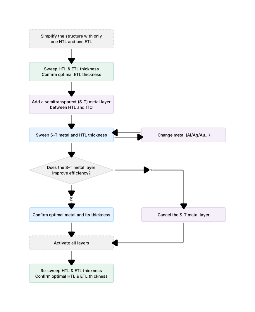
Optimization Process
Taking the bottom-emission structure Substrate/ITO/HTL/EML/ETL/Metal as an example, the following experience-based optimization process is used to enhance the microcavity:
- Simplify the structure (optional): Activate only one HTL and one ETL, uncheck other transport layers.
- Sweep HTL and ETL thickness to confirm the thickness of the layer (traditional bottom-emission structure is ETL) between the emitter and the total reflective metal electrode at optimal efficiency, and enter this value into the Structure.
- Add a semitransparent metal layer between HTL and ITO, and sweep the thickness of the metal and HTL.
- Replace the metal material (Al/Ag/Au) and repeat the previous step to find the most suitable metal material (if all metals lead to efficiency reduction, the structure is not suitable for the strong microcavity with dual metal layers).
- Confirm the optimal thickness of the semitransparent metal layer and enter it into the Structure.
- Re-sweep HTL and ETL thickness to confirm the maximum efficiency improvement compared to when there is no semitransparent metal layer.
- Activate all the layers not activated in step 1, and explore whether these layers affect the microcavity.