
Optical Model and Principles
Model Applicability
Simulation models are used to imitate how real-world objects and systems behave. Every simulation model has a specific range of applicability. Within this range, simulations can more accurately reflect real-world conditions. Outside this range, certain errors may be introduced, or the simulation may fail to represent reality.
Therefore, before using a simulation model, carefully consider whether your project is suitable for the simulation, rather than prematurely concluding that “the simulation model is inaccurate.”
The simulation model used by Leda is invented by Prof. Kristiaan Neyts. It has been validated in the OLED field for over 20 years and has become the industry standard for OLEDs. It is also applicable to QLEDs and some PeLEDs. This model assumes that each layer in an OLED is a flat thin film, and the device area is significantly larger than the thickness of the functional layers, excluding the substrate (i.e., a large width-to-height ratio), using a dipole as the emission model. If your device has a large thickness and limited area, some optical effects at the edges may not be simulated by Leda.
Leda’s model is based on the following assumptions and conditions:
- The emission layer (EML) is transparent and does not absorb the light it emits (the emission spectrum and absorption spectrum do not overlap or overlap very slightly).
- Each layer of the structure is flat, and the interface transitions are clear, meaning there is almost no mixing of two materials at the interface.
- The emitter can be regarded as an ideal point dipole.
- There is at least a wavelength/50 distance between the dipole and the absorbing medium.
- There are no magnetic materials, i.e., the relative permeability is 1 (this is generally not a concern as most materials meet this criterion).
- There are no optical gain materials, meaning the overall structure is optically lossy.
Model and Experimental Discrepancies
There is always a discrepancy between simulation results and experimental results; perfect alignment is nearly impossible. The discrepancies mainly arise from the following aspects:
- Approximations or fittings in the simulation model. Approximations introduced to handle complex situations in the model can cause some errors.
- Input parameters in simulation do not match reality. It’s unrealistic to expect accurate outputs from incorrect inputs.
- Insufficient precision of experimental devices. For instance, the simulation model requires flat surfaces for each layer, but due to process reasons, the experimental device surfaces may be relatively rough.
- Measurement methods that do not conform to standards. For example, the simulation’s external quantum efficiency (EQE) is defined for light emitted in the forward hemisphere, while the experimental EQE might be measured using a single-angle measurement and Lambertian fitting, or by placing the entire device in an integrating sphere, which does not align with the simulation’s definition and cannot be fitted with simulated data.
- Measurement instrument errors. Insufficient precision of measurement instruments or uncalibrated measurement instruments.
Optical Properties and Effects
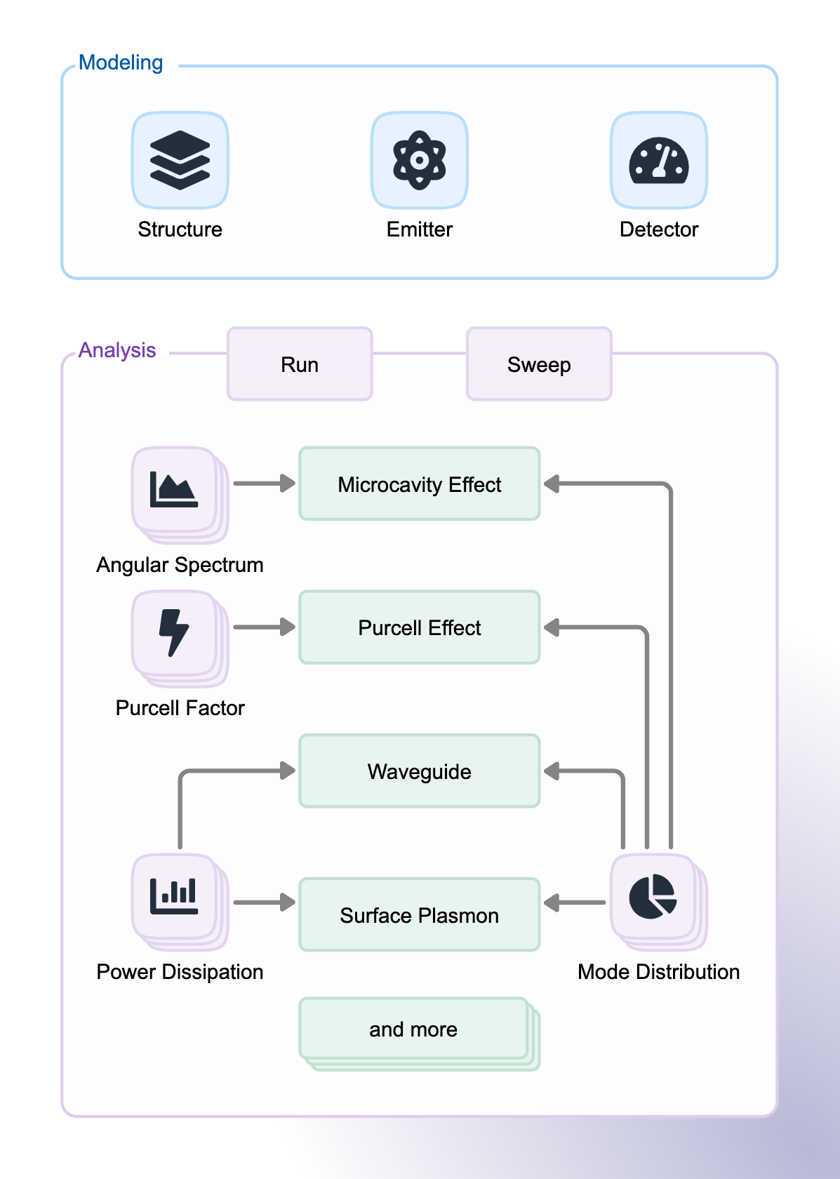
Currently, Leda can simulate the following properties, allowing a comprehensive exploration of the optical effects of OLED/QLEDs.
| Optical Property | Description | Measurable by Experimental Methods |
|---|---|---|
| Spectrum | Intensity distribution with wavelength | Yes |
| Angular Intensity Distribution | Intensity distribution with angle | Yes |
| Power Dissipation | Dissipated power distribution with plane wave vector | No |
| Optical Mode | Optical loss channel distribution | No |
| Purcell Factor | Property related to spontaneous emission, affecting internal quantum efficiency (IQE) | Difficult |
Leda’s model covers a variety of optical effects including Microcavity effect, Purcell effect, Planar waveguide, Optical tunneling, and Surface plasmon polariton, as illustrated below in the combination of optical properties to investigate various optical effects.
Dipole Approximation
The emitter within the emission layer can be represented by a dipole. If the emission materials in OLED and QLED are not regulated for material orientation, they generally emit light isotropically, meaning the radiation power density K is the same in all directions in three-dimensional space. Isotropic emission can be represented by the weighted radiation of dipoles oscillating in the x-y-z directions:
where the subscript iso represents isotropic, v represents the vertical direction, i.e., the z-axis, and h represents the horizontal direction, i.e., the x and y axes.
The radiation field cross-section emitted by a vertically oscillating dipole is shown below:
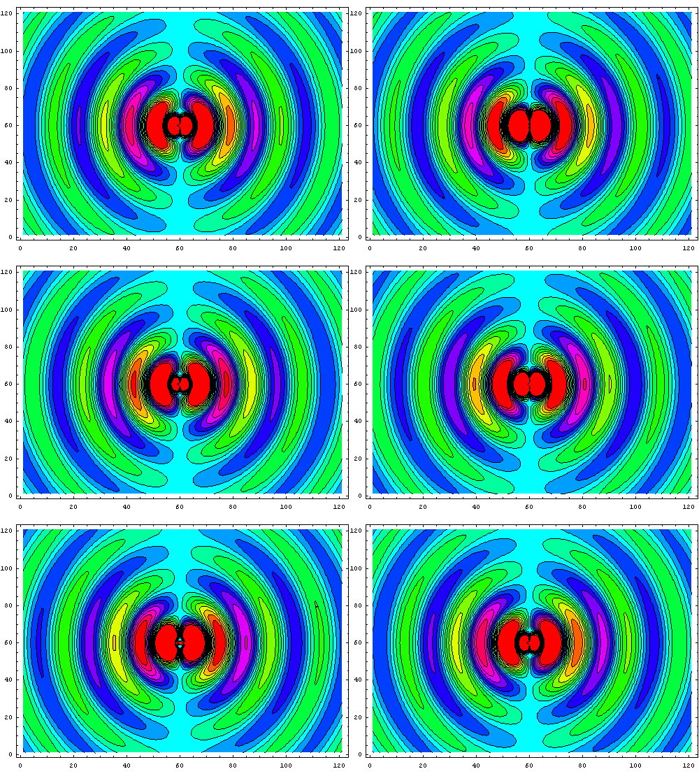
Electric field of a vertically oscillating electric dipole
Source: Author: Loodog

As observed in the above figure, the far-field energy emitted by a vertically oscillating dipole primarily propagates horizontally, with no far-field radiation in the vertically direction. Similarly, a horizontally oscillating dipole primarily radiates in the vertical direction.
The relationship between radiation power and angle is shown below:
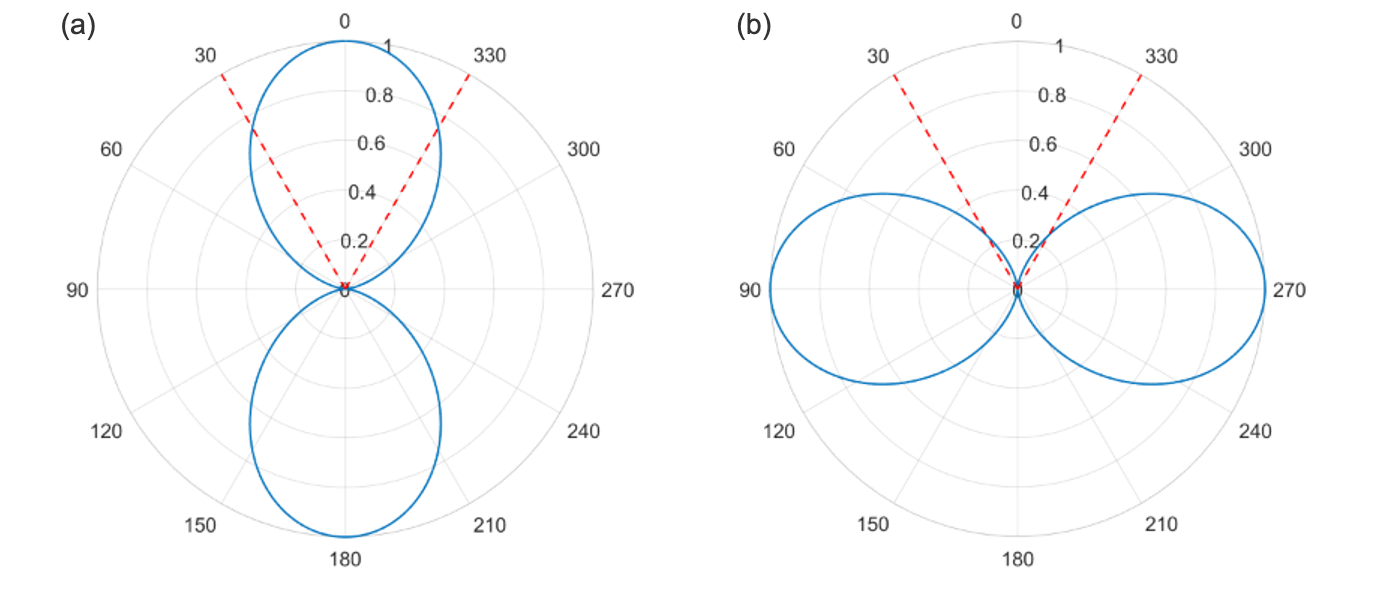
(a) Horizontal dipole and (b) Vertical dipole radiation power (blue line) versus angle; the red dashed line represents the critical angle for total internal reflection.
Since the refractive index of the emission layer is higher than that of air, total internal reflection occurs, preventing light beyond the critical angle from entering the air. As shown in the figure, horizontal dipoles have more energy within the escape angle, resulting in a light extraction efficiency (LEE) significantly greater than that of vertical dipoles, where most energy ultimately becomes loss.
Light Extraction and Loss Mechanisms
External Quantum Efficiency (EQE)
In OLEDs, EQE is defined as:
- IQE is the internal quantum efficiency
- LEE is the light extraction efficiency
is the charge carrier balance factor, describing how many of the injected charges form excitons is the spin formation ratio, the proportion of excitons allowed for radiative decay by spin statistics. If singlet and triplet states form completely randomly, only a quarter of the excitons are singlet excitons capable of emitting fluorescence, i.e., is the effective quantum efficiency or effective radiative efficiency. The relationship between effective quantum yield and intrinsic quantum efficiency is detailed in the Purcell Effect
For QLEDs and PeLEDs, since there is no spin formation ratio, EQE simplifies to:
Light Extraction Efficiency (LEE)
OLED/QLED/PeLED have layered structures, and due to the refractive index difference between materials and air, total internal reflection occurs, confining some light within the device. Light extraction efficiency (LEE) is defined as the “number of photons entering the environment/number of photons emitted by the emission layer.”
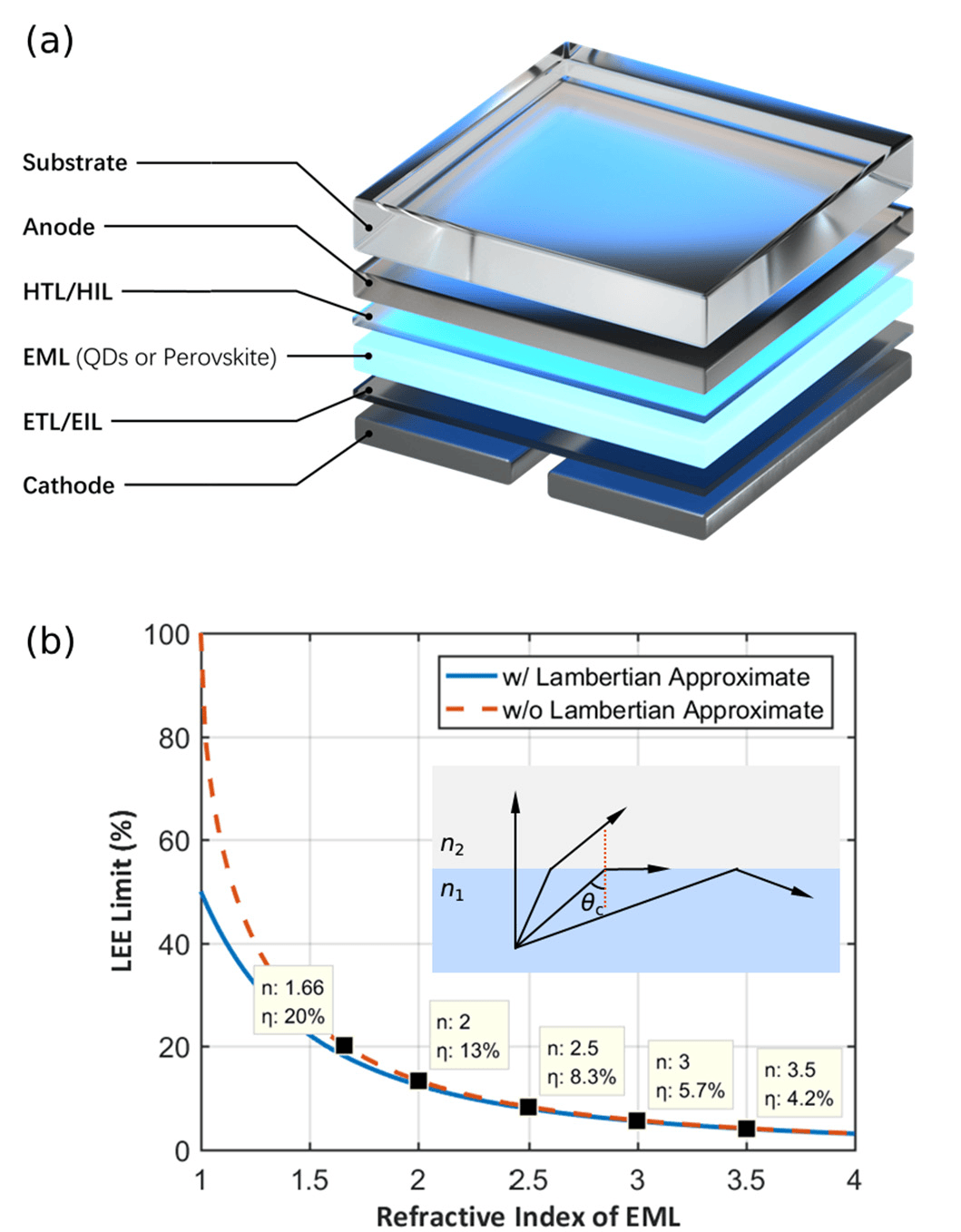
(a) Schematic of bottom-emitting device structure (b) Relationship between light extraction efficiency and emission layer refractive index described by geometrical optics
When the device emission conforms to Lambertian radiation, LEE can be described by the following formula:
According to this formula, the higher the refractive index of the emission layer, the lower the LEE. For example, the refractive index of the emission layers in QLEDs and PeLEDs is higher than that of organic materials in OLEDs, potentially leading to lower efficiency limits.
However, the above “total internal reflection determines light extraction efficiency” perspective only considers geometrical optics based on Snell’s Law. Given the micro-nano scale thickness of the device, additional effects such as microcavity effects, Purcell effects, waveguides, and surface plasmon polaritons exist internally. Therefore, geometrical optics is insufficient for such loss analysis, necessitating more precise wave optics models for simulation. Fortunately, Leda is capable of simulating these effects.
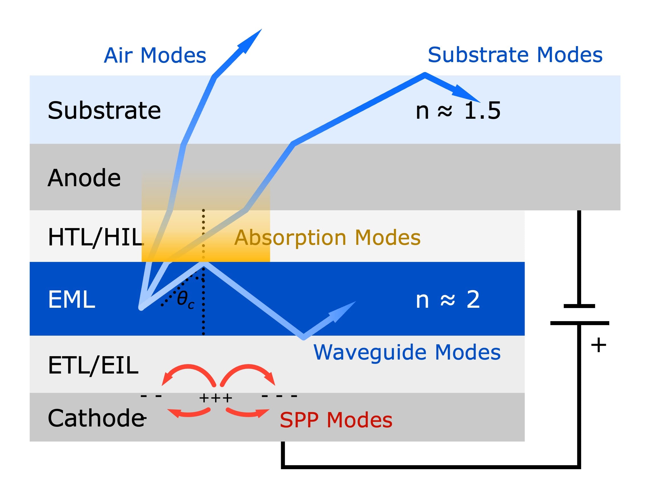
Schematic of optical losses in bottom-emitting devices
Source: DOI: 10.1063/5.0084416
Microcavity Effect
The microcavity effect refers to the formation of microcavities in the OLED layered structure, resulting in internal interference. The term “cavity” implies a planar structure with reflective interfaces, while “micro” indicates that the cavity is on a micro-nano scale, allowing for significant interference on the wavelength scale.
Interference in microcavities is categorized into wide-angle interference and multiple-beam interference, as shown below.
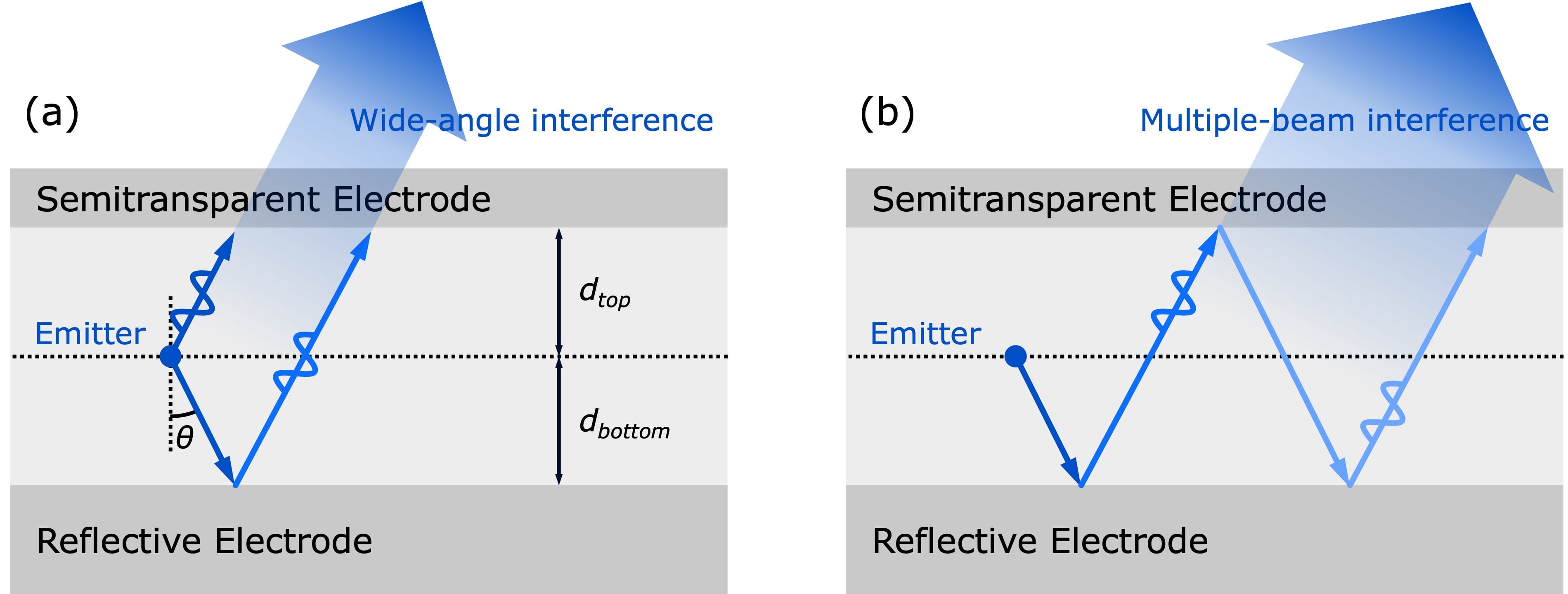
(a) Wide-angle Interference and (b) Multiple-beam Interference in the microcavity
Source: DOI: 10.1109/jphot.2022.3159278
- Wide-angle interference: Interference between light directly emitted by the emitter and reflected light, related to the distance between the emitter and the reflective interface (primarily related to
due to the high reflectivity of the bottom reflective surface).
- Multiple-beam interference: Interference occurring during multiple reflections of light within the device, related to the cavity length (
+ ).
Waveguide
Light undergoing total internal reflection forms waveguides due to interference, eventually converting into thermal loss. Waveguide losses typically account for 30-70% of total losses, thus reducing waveguide modes is a key to enhancing LEE.
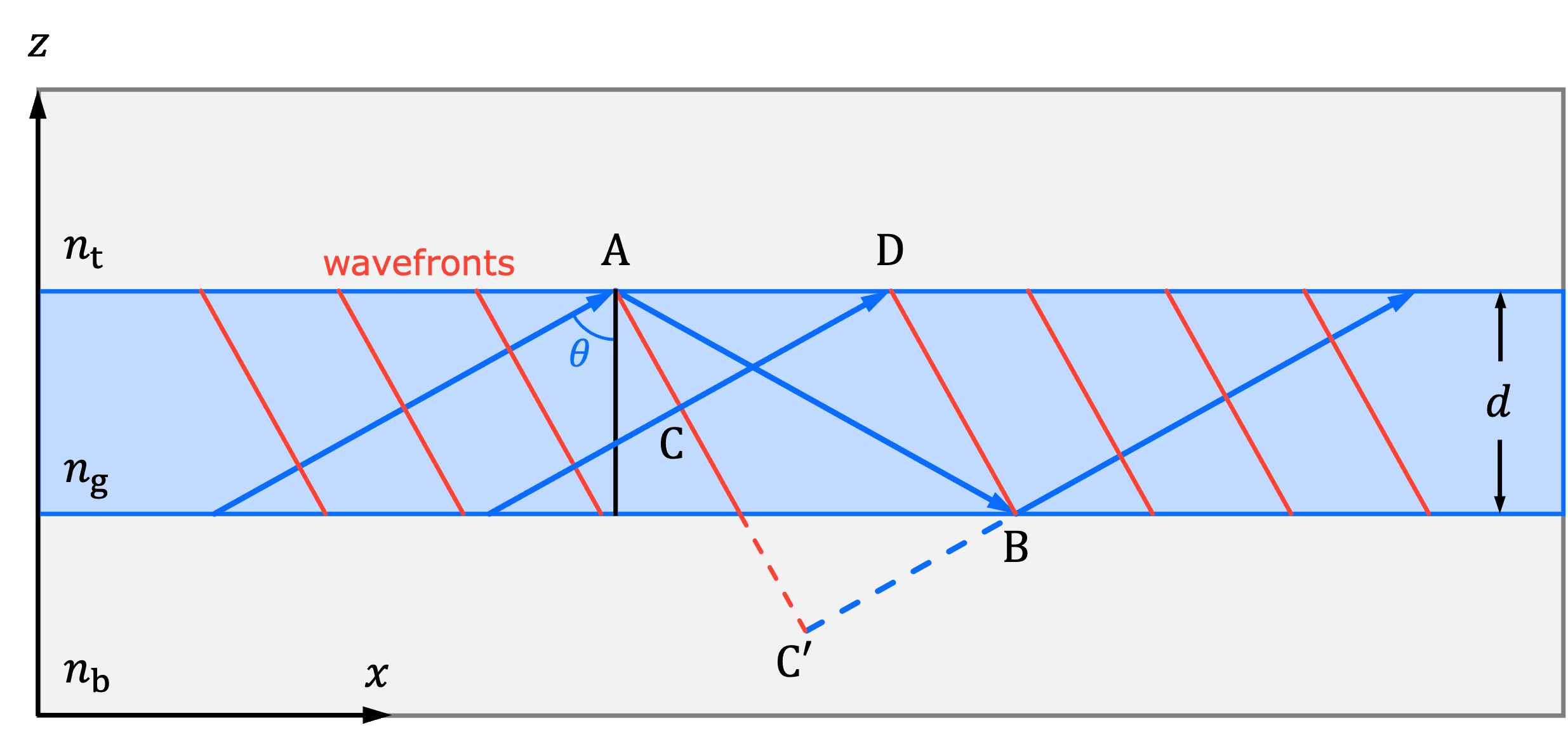
Schematic of a three-layer planar waveguide
The formula for waveguide formation is as follows:
This indicates that waveguide formation is related to cavity length
Surface Plasmon Polariton (SPP)
According to the CPS (Chance, Prock, and Silbey) theory, when an emitter is close to a metal-dielectric interface, energy can be coupled into surface plasmon polaritons (SPPs) through the near field, resulting in non-radiative losses and a reduction in fluorescent lifetime, potentially approaching zero.
According to the Drude model, the resonance frequency of SPPs is related to the refractive indices of the metal and the dielectric. For a given material, wavelength, distance between the dipole and the metal interface, and dipole orientation are key factors in controlling SPP losses.
Since TM-polarized light is a prerequisite for exciting surface plasmon polaritons, and light emitted by vertical dipoles is entirely TM-polarized, vertical dipoles are the main source of SPP losses.
Purcell Effect
Before the Purcell effect was proposed, spontaneous emission was considered an inherent property of atoms or molecules. The Purcell effect describes how the environment (device structure) can regulate spontaneous emission. By leveraging the Purcell effect, we can enhance quantum efficiency through device structure optimization.
The relationship between the Purcell factor and the radiative decay rate is given by:
where
When the intrinsic quantum efficiency
The relationship between the Purcell factor and quantum efficiency is:
where
Dipoles with different orientations have different Purcell factors
Electrical and Non-Radiative Losses
In general, LED emission undergoes three processes: “charge injection and exciton formation → electro-optical conversion → optical loss and extraction,” as detailed in External Quantum Efficiency (EQE). Leda is an optical simulation software and does not include electrical or material simulations. The first two steps are outside the scope of Leda’s simulations but can serve as inputs to Leda’s optical model.
- The charge carrier balance factor
and spin formation ratio are inputs to Leda’s Conversion Efficiency, which is not affected by the Purcell effect. - The intrinsic quantum yield
is input to Leda’s Quantum Efficiency, which is regulated by the Purcell effect. By inputting the intrinsic quantum yield, the model considers the impact of the microcavity on quantum efficiency, ultimately outputting the effective quantum efficiency .
Loss Analysis Methods
Complex mechanisms of light extraction and loss cannot be described by geometrical optics. We will use Mode distribution based on in-plane wave vector to analyze optical losses.
Power Dissipation
The in-plane wave vector
where
where
We introduce the definitions of
The relationship between
When
It implies
Under the influence of optical effects such as microcavity and waveguide, the energy of light will be distributed with
In the diagram below, different modes are defined based on the relationship between
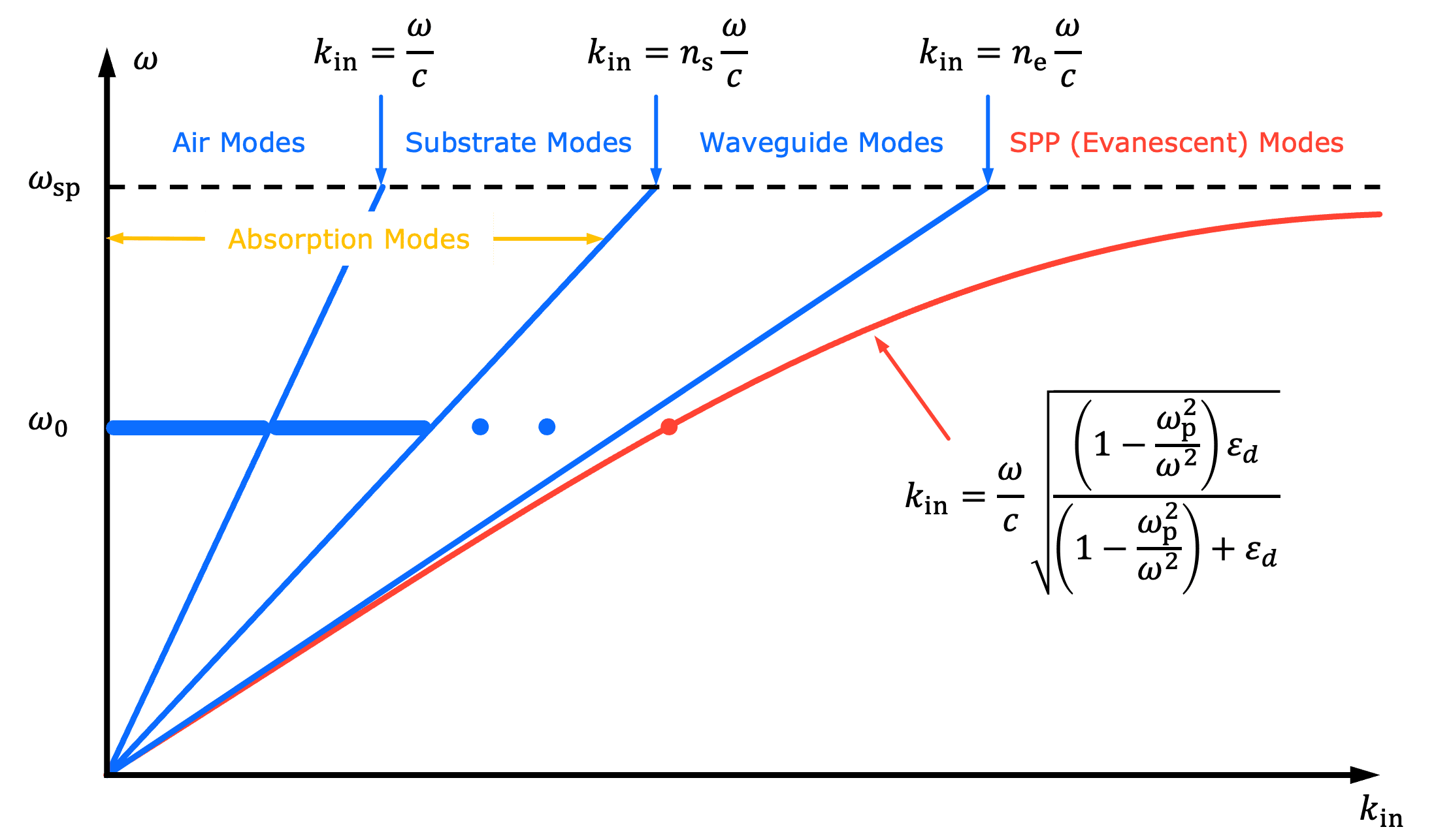
Schematic of dispersion relation
When the frequency of light is
Optical Mode
The simple discussion above divides
In Leda, energy distribution in different modes can be calculated using Mode detectors.
| Mode Name in Leda | Scientific Mode Name | Common Description (Not Definition) | |
|---|---|---|---|
| TOC | top-outcoupled | ||
| BOC | bottom-outcoupled | ||
| TOC (Top Layer is Air) | Air Mode | Light extraction efficiency / Outcoupling efficiency | |
| SUB (Top Layer is Air) | Substrate Mode | Light confined in the substrate due to reflection at the substrate-air interface | |
| ABS (No Incoherent Layer) | Absorption Mode | Absorption loss in the TOC path | |
| ABS (With Incoherent Layer) | Absorption Mode | Absorption loss in TOC and SUB paths | |
| WVG (No Incoherent Layer) | Waveguide Mode | Waveguide loss due to total internal reflection and interference | |
| WVG (With Incoherent Layer) | Waveguide Mode | Waveguide loss due to total internal reflection and interference | |
| EVA | Evanescent Mode | Evanescent wave loss, generally refers to SPP loss | |
| NRA | Nonradiative Mode | Non-radiative loss, occurs when quantum efficiency is not 100% |
Air mode corresponds to EQE. When both Conversion Efficiency and Quantum Efficiency are 1 (default setting), Air mode corresponds to LEE.